Close Menu
    Login
    • Register
    • Log in
    • Entries feed
    • Comments feed
    • WordPress.org
    • Home
    • Technology
    • Daily Tech
      • Science and Technology
    • Gadgets
    • Gaming
    • Space Exploration
    • Scope
    • Tech News
    Facebook X (Twitter) Instagram Pinterest YouTube WhatsApp
    Facebook X (Twitter) Instagram
    NewTechMania | Tech Revolution Mastering The InsightsNewTechMania | Tech Revolution Mastering The Insights
    Login
    • Home
    • Blog
    • Gadgets
      • Gaming
    • Technology
      • Science
    • Automobile
    • Exploration
    • Scope
    • Tech News
    NewTechMania | Tech Revolution Mastering The InsightsNewTechMania | Tech Revolution Mastering The Insights
    You are at:Home»Technology»TSMC Declares It Will Start Manufacturing 1nm Transistors in 2030 – technology
    Technology

    TSMC Declares It Will Start Manufacturing 1nm Transistors in 2030 – technology

    By Karan sharma29 December 2023No Comments3 Mins Read
    Facebook Twitter Pinterest LinkedIn Tumblr Email
    1nm Carbon Nanotube transistor
    1nm Carbon Nanotube transistor
    Share
    Facebook Twitter LinkedIn Pinterest Email

    The business added that by then, it anticipates having one trillion transistors on a single package.

    The Taiwan Semiconductor Manufacturing Corporation (TSMC) has recently revised its plan, which outlines the company’s objectives for the semiconductor industry until the year 2030 and beyond. In a way, it is similar to a corporate vision board, in that it displays the company’s intentions for ambitious designs that will enable the use of up to one trillion transistors in a single package. It also highlighted its aspirations to eventually arrive at a watershed measure in semiconductor manufacturing, which is the fabrication of 1nm transistors. This was one of the things that it highlighted at the same time.

    At the most recent IEDM conference, the corporation presented its plans and produced a roadmap that outlined its plans for the future. Other plans were also presented. There are some genuinely tantalising chips at the very end of the road, and TSMC has stated that it will be possible to place a trillion chips on a package by using several chiplets that are stacked within a three-dimensional space. Coincidentally, Intel has also indicated in the past that it believes it should be possible to have one trillion transistors on a package by the year 2030. To fit a trillion transistors on a device, the company’s CEO, Pat Gelsinger, stated last year that the company plans to use chiplets and sophisticated packaging technologies. Additionally, the company plans to use chiplets, which are referred to as tiles in Intel nomenclature.

    images 1 4 1
    By 2030, TSMC predicts reaching 1 nm transistors, which will enable up to 200 billion of them to be produced on a single monolithic die. Credit: TSMC

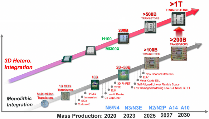
    In addition, TSMC revealed that monolithic designs have the potential to reach 200 billion transistors by the year 2030. To provide some background, the H100, which contains 80 billion transistors, is currently Nvidia’s largest monolithic TSMC die currently available. At the same time, the designs of the chiplets that are currently being used are also becoming quite huge. For example, Intel’s Ponte Vecchio has 100 billion transistors, and AMD’s new MI300 has 146 billion transistors.

    According to Tom’s Hardware, in order for TSMC to achieve these objectives, the company will first move to a 2nm process, and then eventually move on to transition to both 1.4nm and 1nm nodes. It appears from the plan that it will continue to use the 3nm technology until the year 2025, after which it will begin production using the 2nm technology. With the arrival of the 1nm A10 node in 2023, it is anticipated that it will be on a 1.4nm A14 process by the year 2028.

    One of the most intriguing aspects of this schedule is that Intel has already begun making preparations to manufacture its very own 2nm technology, which it refers to as Intel 20A, in the year 2024. Next, it is anticipated that it would develop to 1.8nm, also known as Intel 18A, in the year 2025. As is customary with Intel, we will have to wait and see if it is able to meet those targets; nevertheless, the company has stated that it is still functioning according to the timetable. In the event that Intel is successful in manufacturing a 20A central processing unit (CPU) in 2024, which is referred to as Arrow Lake, the business will theoretically have leapfrogged TSMC for the first time in a very long time. This was the company’s objective all along with its “five nodes in four years” plan that started in 2021.

    Share. Facebook Twitter Pinterest LinkedIn Tumblr Email
    Previous ArticleResearchers Studying Security Exposes a Four-Year iPhone Backdoor Hacking Scheme – technology
    Next Article Google consents to resolve a $5 billion lawsuit alleging that it tracked users using Incognito mode – technology

    Related Posts

    Skypeaklimits 2024: Your Digital Success Elevate Your Presence

    OpenAI partners with Palmer Luckey’s Anduril to build military AI

    MS assures Windows 11 TPM security requirement won’t change

    Peloton launches audio-focused strength training app

    Add A Comment

    Comments are closed.

    • Recent Posts
    20 December 2024

    What is the Best Tech News Site? 2025

    20 December 2024

    How to Stay Updated With Tech News 2024

    5 December 2024

    Skypeaklimits 2024: Your Digital Success Elevate Your Presence

    5 December 2024

    OpenAI partners with Palmer Luckey’s Anduril to build military AI

    5 December 2024

    MS assures Windows 11 TPM security requirement won’t change

    5 December 2024

    Peloton launches audio-focused strength training app

    5 December 2024

    Bitcoin crosses $100,000 for the first time

    2 December 2024

    Musk asks court to prohibit OpenAI from going for-profit

    NewTechMania Tech Revolution Mastering Insights Embark on a tech adventure with latest gadgets technologies join us exploring possibilities main logo

    About US

    Embark on a tech adventure with NewTechMania. From the latest gadgets to emerging technologies, join us in exploring the possibilities that lie ahead.

    Terms

    • Privacy
    • Cookie
    • Terms
    • Disclaimer
    • DMCA

    Useful Links

    • Home
    • About Us
    • Contact Us
    • Get In Touch
    • Privacy

    Weekly Newslatter

    Subscribe to our newsletter to get updated!
    © 2024 NewTechMania. All RightS Reserved.
    Facebook-f Twitter Instagram Pinterest Youtube

    Type above and press Enter to search. Press Esc to cancel.

    Sign In or Register

    Welcome Back!

    Login below or Register Now.

    Continue with Google
    Lost password?

    Register Now!

    Already registered? Login.

    Continue with Google

    A password will be e-mailed to you.