By 2024, the company’s V9 semiconductors might enable reasonably priced, large-capacity drives.
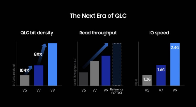
Those that make memories are getting ready to gather at an international conference in order to showcase their most recent accomplishments, and it would appear that Samsung will be taking home at least one prize from the event. The business is getting ready to make the announcement that it has produced 280-layer QLC NAND flash, which will enable it to outperform its competitors in terms of chip density by as much as fifty percent. The introduction of this NAND in 2024 could open the way for high-capacity solid-state drives that are also inexpensive.
It is expected that Samsung’s presentation at the International Solid-State Circuits Conference (ISSCC), which will begin on February 20th, will be a barnburner, as stated by Computerbase in Germany. There is a presentation that is going to be given on the topic of “A 280-Layer 1Tb 4b/cell 3D-NAND Flash Memory with a 28.5Gb/mm2 Areal Density and a 3.2GB/s High-Speed IO Rate.” Even if that is a lot to decipher, the most important figures are the 280 layers and the 28.5Gb/mm2 density, which is a new record for the industry. The Chinese memory manufacturer YMTC, which presently produces 232-layer NAND at just 19.8 gigabytes per millimeter squared, will be dethroned as a result of its arrival.

Not even SK Hynix and Micron, two companies that are well-known in the flash industry, are capable of surpassing this accomplishment. There is a 300-layer TLC NAND memory available from SK Hynix, although it supports only 20Gb/mm2. PLC NAND, which employs five bits per cell, is another technology that Intel is working on. However, even this feat only brings the total capacity to 23.3 gigabytes per millimeter2. With a maximum capacity of 14.6 gigabytes per square millimeter, Micron is promoting their 232-layer TLC NAND. The sole drawback to this innovation by Samsung is that it is unable to carry out prolonged data transfers at maximum speed. This is because QLC drives use an SLC buffer, which prevents them from supporting such transfers. The speed of the system significantly decreases after that buffer is filled. Because of this, QLC NAND drives are more concerned with capacity than performance; hence, it is highly unlikely that we will see this on PCIe 5.0 drives for our gaming rigs.
There is a high probability that Samsung’s next-generation VNAND will be a component of its V9 series, also known as ninth-generation flash. As a result of the fact that its V8 technology consists of 238 layers, it is presumed that 280 layers be V9 models. Computerbase reports that Samsung had previously announced V9 QLC NAND for the year 2024, but with a transfer speed of 2.4 gigabits per second. In its future presentation, it will be stated that the speed has climbed to 3.2 gigabits per second, which indicates that the company may have surpassed its goals.
In order to determine what kinds of capacities this kind of density is capable of affording, we will have to wait a few weeks, although Tom’s Hardware is speculating that it could lead to M.2 drives with capacities of 8TB and 16TB eventually. Because Samsung has not yet released anything for a consumer drive that is larger than 4 terabytes, the company’s V9 technology may result in a paradigm shift in the capacity of consumer solid-state drives (SSDs).

